- 您现在的位置:买卖IC网 > Sheet目录484 > NOIH2SM1000S-HHC (ON Semiconductor)IC SPACE IMAGE SENSOR 84-JLCC
NOIH2SM1000A
TABLES AND FIGURES
Specification Tables
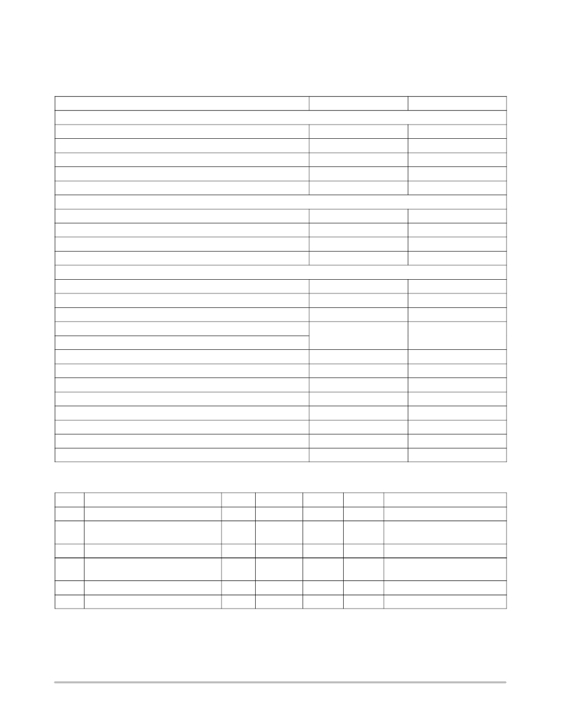
Table 10. TYPE VARIANT SUMMARY
HAS2 Type Variants
Optical quality (see Optical Quality ? Definitions on page 67)
Dead pixels
Bright pixels in FPN image
Bad pixels in PRNU image
Bad columns
Bad rows
Bright pixel clusters
2 adjacent bright pixels
4 or more adjacent bright pixels
DSNU defects at 22 dec BOL
DSNU defects at 22 dec EOL
Particle contamination
Fixed particles outside focal plane
Mobile particles > 20 m m
Fixed particles on focal plane > 20 m m
Mobile particles > 10 m m and < 20 m m
Fixed particles on focal plane > 10 m m and < 20 m m
Particles < 10 m m
Wafer lot acceptance (see section Wafer Lot Acceptance on page 6)
Glass lot acceptance (see section Glass Lot Acceptance on page 6)
Assembly lot acceptance (Table 7 on page 6)
Periodic testing (Table 8 on page 7)
Screening (Table 9 on page 7)
Calibration data
Visual Inspection + particle mapping
Table 11. MAXIMUM RATINGS
Engineering Model
100
50
150
5
5
25
10
1200
1500
N/A
0
0
20
N/A
NO
NO
NO
NO
NO
NO
NO
Flight Model
20
20
50
0
0
2
0
1000
1250
N/A
0
0
10
N/A
Yes
Yes
Yes
Yes
Yes
Yes
Yes
No.
1
2
3
4
5
6
Characteristic
Any supply voltage except VDD_RES
Supply voltage at VDD_RES
Voltage on any input terminal
Soldering temperature
Operating temperature
Storage temperature
Min
–0.5
–0.5
–0.5
NA
–40
–55
Typ
3.3
3.3
3.3
NA
NA
NA
Max
+7.0
+5.0
Vdd + 0.5
260
+85
+125
Unit
V
V
V
° C
° C
° C
Remarks
3.3 V for normal operation; up to
5 V for increased full well capacity.
Hand soldering only; See Solder-
ing Instructions on page 1
Stresses exceeding Maximum Ratings may damage the device. Maximum Ratings are stress ratings only. Functional operation above the
Recommended Operating Conditions is not implied. Extended exposure to stresses above the Recommended Operating Conditions may affect
device reliability.
http://onsemi.com
9
发布紧急采购,3分钟左右您将得到回复。
相关PDF资料
NOII5SM1300A-QDC
SENSOR IMAGE MONO CMOS 84-LCC
NOIL1SC4000A-GDC
IC IMAGE SENSOR 4MP 127-PGA
NOIL1SE3000A-GDC
IC IMAGE SENSOR 3MP 369-PGA
NOIL1SM0300A-WWC
IC IMAGE SENSOR LUPA300 48LLC
NOIL2SC1300A-GDC
IC IMAGE SENSOR LUPA1300 168PGA
NOIV1SE025KA-GDC
IC IMAGE SENSOR 25MP 355PGA
NP100P04PDG-E1-AY
MOSFET P-CH -40V MP-25ZP/TO-263
NP100P04PLG-E1-AY
MOSFET P-CH -40V MP-25ZP/TO-263
相关代理商/技术参数
NOII4SM1300A-QDC
功能描述:SENSOR IMAGE MONO CMOS 84-LCC RoHS:否 类别:传感器,转换器 >> 图像,相机 系列:- 标准包装:480 系列:- 象素大小:6.7µm x 6.7µm 有源象素阵列:768H x 488V 每秒帧数:52 电源电压:3.3V 类型:CMOS 成像 封装/外壳:48-QFP 供应商设备封装:48-QFP 包装:托盘 请注意:* 配用:4H2105-ND - HEADBOARD FOR KAC-004014H2104-ND - KIT EVAL FOR KAC-00401 其它名称:4H20954H2095-NDKAC-00401-CBC-LB-A0
NOII4SM1300A-QWC
功能描述:SENSOR IMAGE MONO CMOS 84-LCC RoHS:否 类别:传感器,转换器 >> 图像,相机 系列:- 标准包装:480 系列:- 象素大小:6.7µm x 6.7µm 有源象素阵列:768H x 488V 每秒帧数:52 电源电压:3.3V 类型:CMOS 成像 封装/外壳:48-QFP 供应商设备封装:48-QFP 包装:托盘 请注意:* 配用:4H2105-ND - HEADBOARD FOR KAC-004014H2104-ND - KIT EVAL FOR KAC-00401 其它名称:4H20954H2095-NDKAC-00401-CBC-LB-A0
NOII4SM6600A-QDC
功能描述:图像传感器和彩色传感器 IBIS4-6600 MONO LLC68 RoHS:否 制造商:Avago Technologies 类型:Color Sensors 工作电源电压:2.5 V 封装 / 箱体: 图象大小: 颜色读出:Color 最大工作温度:+ 70 C 最小工作温度:- 25 C 封装:Reel
NOII5FM1300A-QDC
功能描述:SENSOR IMAGE 1.3MP CMOS 84-LCC RoHS:否 类别:传感器,转换器 >> 图像,相机 系列:- 标准包装:480 系列:- 象素大小:6.7µm x 6.7µm 有源象素阵列:768H x 488V 每秒帧数:52 电源电压:3.3V 类型:CMOS 成像 封装/外壳:48-QFP 供应商设备封装:48-QFP 包装:托盘 请注意:* 配用:4H2105-ND - HEADBOARD FOR KAC-004014H2104-ND - KIT EVAL FOR KAC-00401 其它名称:4H20954H2095-NDKAC-00401-CBC-LB-A0
NOII5SC1300A-QDC
功能描述:SENSOR IMAGE COLOR CMOS 84-LCC RoHS:否 类别:传感器,转换器 >> 图像,相机 系列:- 标准包装:480 系列:- 象素大小:6.7µm x 6.7µm 有源象素阵列:768H x 488V 每秒帧数:52 电源电压:3.3V 类型:CMOS 成像 封装/外壳:48-QFP 供应商设备封装:48-QFP 包装:托盘 请注意:* 配用:4H2105-ND - HEADBOARD FOR KAC-004014H2104-ND - KIT EVAL FOR KAC-00401 其它名称:4H20954H2095-NDKAC-00401-CBC-LB-A0
NOII5SM1300A-QDC
功能描述:SENSOR IMAGE MONO CMOS 84-LCC RoHS:否 类别:传感器,转换器 >> 图像,相机 系列:- 标准包装:480 系列:- 象素大小:6.7µm x 6.7µm 有源象素阵列:768H x 488V 每秒帧数:52 电源电压:3.3V 类型:CMOS 成像 封装/外壳:48-QFP 供应商设备封装:48-QFP 包装:托盘 请注意:* 配用:4H2105-ND - HEADBOARD FOR KAC-004014H2104-ND - KIT EVAL FOR KAC-00401 其它名称:4H20954H2095-NDKAC-00401-CBC-LB-A0
NOIL1SC4000A-GDC
功能描述:IC IMAGE SENSOR 4MP 127-PGA RoHS:是 类别:传感器,转换器 >> 图像,相机 系列:* 标准包装:480 系列:- 象素大小:6.7µm x 6.7µm 有源象素阵列:768H x 488V 每秒帧数:52 电源电压:3.3V 类型:CMOS 成像 封装/外壳:48-QFP 供应商设备封装:48-QFP 包装:托盘 请注意:* 配用:4H2105-ND - HEADBOARD FOR KAC-004014H2104-ND - KIT EVAL FOR KAC-00401 其它名称:4H20954H2095-NDKAC-00401-CBC-LB-A0
NOIL1SE0300A-QDC
功能描述:SENSOR IMAGE COLOR CMOS 48-LCC RoHS:否 类别:传感器,转换器 >> 图像,相机 系列:- 标准包装:480 系列:- 象素大小:6.7µm x 6.7µm 有源象素阵列:768H x 488V 每秒帧数:52 电源电压:3.3V 类型:CMOS 成像 封装/外壳:48-QFP 供应商设备封装:48-QFP 包装:托盘 请注意:* 配用:4H2105-ND - HEADBOARD FOR KAC-004014H2104-ND - KIT EVAL FOR KAC-00401 其它名称:4H20954H2095-NDKAC-00401-CBC-LB-A0
